Original Link: https://www.anandtech.com/show/7126/the-arm-diaries-part-2-understanding-the-cortex-a12
The ARM Diaries, Part 2: Understanding the Cortex A12
by Anand Lal Shimpi on July 17, 2013 12:30 PM EST- Posted in
- CPUs
- Arm
- SoCs
- Cortex A12
A couple of weeks ago I began this series on ARM with a discussion of the company’s unique business model. In covering semiconductor companies we’ve come across many that are fabless, but it’s very rare that you come across a successful semiconductor company that doesn’t even sell a chip. ARM’s business entirely revolves around licensing IP for its instruction set as well as its own CPU (and now GPU and video) cores.
Before we get into discussions of specific cores, it’s important to talk about ARM’s portfolio as a whole. In the PC space we’re used to focusing on Intel’s latest and greatest microarchitectures, which are then scaled in various ways to hit lower price targets. We might see different core counts, cache sizes, frequencies and maybe even some unfortunate instruction set tweaking but for the most part Intel will deliver a single microarchitecture to cover the vast majority of the market. These days, this microarchitecture is simply known as Core.
Back in 2008, Intel introduced a second microarchitecture under the Atom brand to target lower cost (and lower power) markets. The combination of Atom and Core spans the overwhelming majority of the client computing market for Intel. The prices of these CPUs range from the low double digits with Atom to many hundreds of dollars for the highest end Core processors (the most expensive desktop Haswell is $350, however mobile now extends up to $1100). There are other designs that target servers (which are then repurposed for ultra high-end desktops), but those are beyond the scope of this discussion for now.
If we limit our discussion to personal computing devices (smartphones, tablets, laptops and desktops), where Intel uses two microarchitectures ARM uses three. The graphic below illustrates the roadmap:
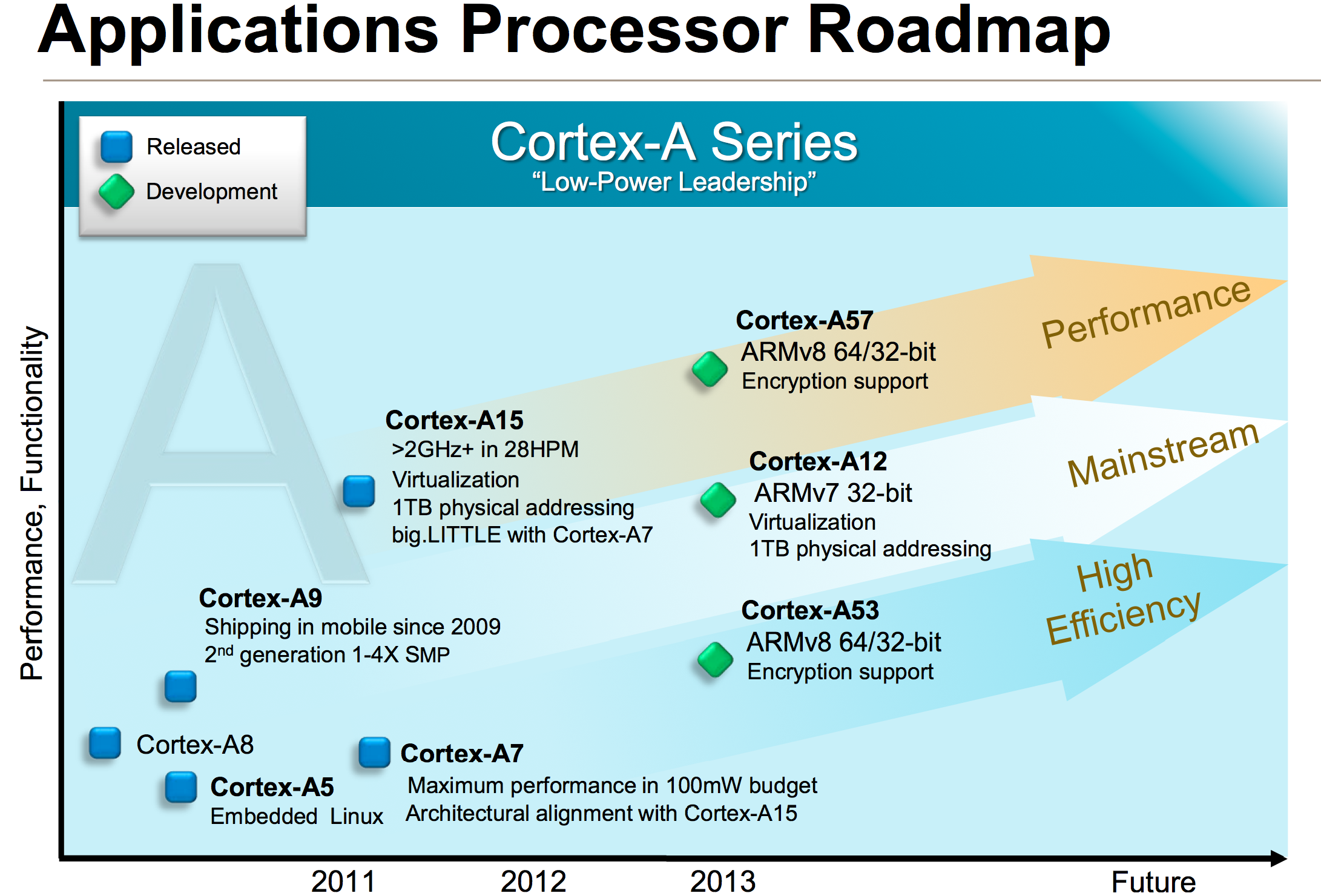
You need to somewhat ignore the timescale on the x-axis since those dates really refer to when ARM IP is first available to licensees, not when products are shipping to consumers, but you get an idea for the three basic vectors of ARM’s Cortex A-series of processor IP. Note that there are also Cortex R (embedded) and Cortex M (microcontroller) series of processor IP offered as well, but once again those are beyond the scope of our discussion here.
If we look at currently available cores, there’s the Cortex A15 on the high end, Cortex A9 for the mainstream and Cortex A7 for entry/low cost markets. If we’re to draw parallels with Intel’s product lineup, the Cortex A15 is best aligned with ultra low power/low frequency Core parts (think Y-series SKUs), while the Cortex A9 vector parallels Atom. Cortex A7 on the other hand targets a core size/cost/power level that Intel doesn’t presently address. It’s this third category labeled high efficiency above that Intel doesn’t have a solution for. This answers the question of why ARM needs three microarchitectures while Intel only needs two: in mobile, ARM targets a broader spectrum of markets than Intel.
Dynamic Range
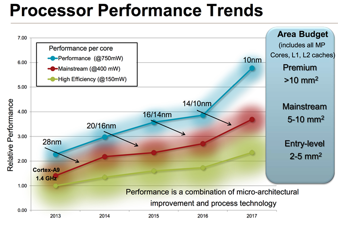
If you’ve read any of our smartphone/tablet SoC coverage over the past couple of years you’ll note that I’m always talking about an increasing dynamic range of power consumption in high-end smartphones and tablets. Each generation performance goes up, and with it typically comes a higher peak power consumption. Efficiency improvements (either through architecture, process technology or both) can make average power in a reasonable workload look better, but at full tilt we’ve been steadily marching towards higher peak power consumption regardless of SoC vendor. ARM provided a decent overview of the CPU power/area budget as well as expected performance over time of its CPU architectures:

Looking at the performance segment alone, we’ll quickly end up with microarchitectures that are no longer suited for mobile, either because they’re too big/costly or they draw too much power (or both).
The performance vector of ARM CPU IP exists because ARM has its sights set higher than conventional smartphones. Starting with the Cortex A57, ARM hopes to have a real chance in servers (and potentially even higher performance PCs, Windows RT and Chrome OS being obvious targets).
Although we see limited use of ARM’s Cortex A15 in smartphones today (some international versions of the Galaxy S 4), it’s very clear that for most phones a different point on the power/performance curve makes the most sense.
The Cortex A8 and A9 were really the ARM microarchitectures that drove smartphone performance over the past couple of years. The problem is that while ARM’s attentions shifted higher up the computing chain with Cortex A15, there was no successor to take the A9’s place. ARM’s counterpoint would be that Cortex A15 can be made suitable for lower power operation, however its partners (at least to date) seemed to be focused on extracting peak performance from the A15 rather than pursuing a conservative implementation designed for lower power operation. In many ways this makes sense. If you’re an SoC vendor that’s paying a premium for a large die CPU, you’re going to want to get the most performance possible out of the design. Only Apple seems to have embraced the idea of using die area to deliver lower power consumption.
The result of all of this is that the Cortex A9 needed a successor. For a while we’d been hearing about a new ARM architecture that would be faster than Cortex A9, but lower power (and lower performance) than Cortex A15. Presently, the only architecture in between comes from Qualcomm in the form of some Krait derivative. For ARM to not let its IP licensees down, it too needed a solution for the future of the mainstream smartphone market. Last month we were introduced to that very product: ARM’s Cortex A12.
Slotting in numerically between A9 and A15, the initial disclosure unfortunately didn’t come with a whole lot of actual information. Thankfully, we now have some color to add.
Introduction to Cortex A12 & The Front End
At a high level ARM’s Cortex A12 is a dual-issue, out-of-order microarchitecture with integrated L2 cache and multi-core capable.
The Cortex A12 team all previously worked on Cortex A9. ARM views the resulting design as not being a derivative of Cortex A9, but clearly inspired by it. At a high level, Cortex A12 features a 10 - 12 stage integer pipeline - a lengthening of Cortex A9’s 8 - 11 stage pipeline. The architecture is still 2-wide out-of-order, but unlike Cortex A9 the new tweener is fully out of order including load/store (within reason) and FP/NEON.

Cortex A12 retains feature and ISA compatibility with ARM’s Cortex A7 and A15, making it the new middle child in the updated microprocessor family. All three parts support 40-bit physical addressing, the same 128-bit AXI4 bus interface and the same 32-bit ARM-v7A instruction set (NEON is standard on Cortex A12). The Cortex A12 is so compatible with A7 and A15 that it’ll eventually be offered in a big.LITTLE configuration with a cluster of Cortex A7 cores (initial versions lack the coherent interface required for big.LITTLE).
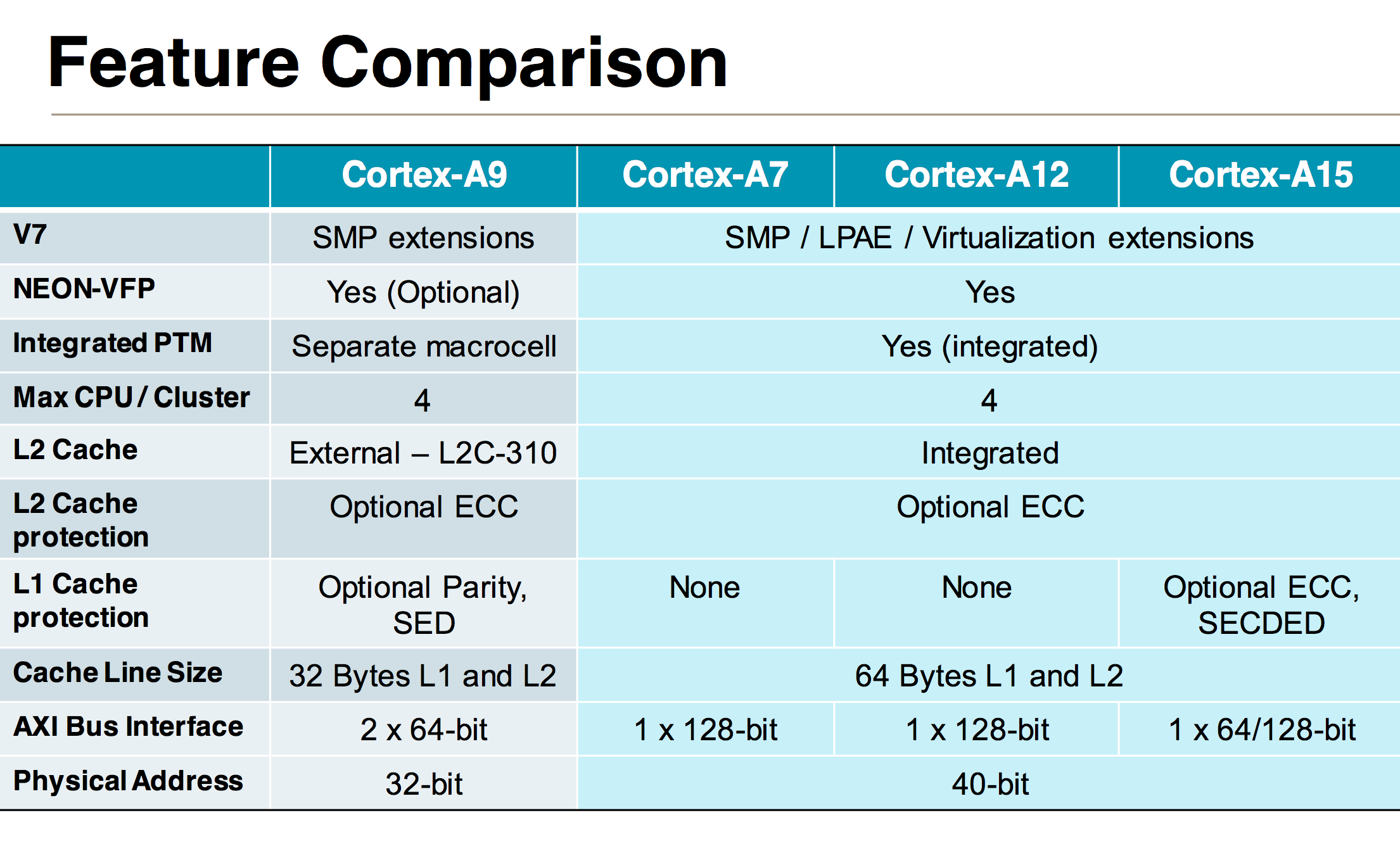
In the Cortex A9, ARM had a decoupled L2 cache that required some OS awareness. The Cortex A12 design moves to a fully integrated L2, similar to the A7/A15. The L2 cache operates on its own voltage and frequency planes, although the latter can be in sync with the CPU cores if desired. The L2 cache is shared among up to four cores. Larger core count configurations are supported through replication of quad-core clusters.
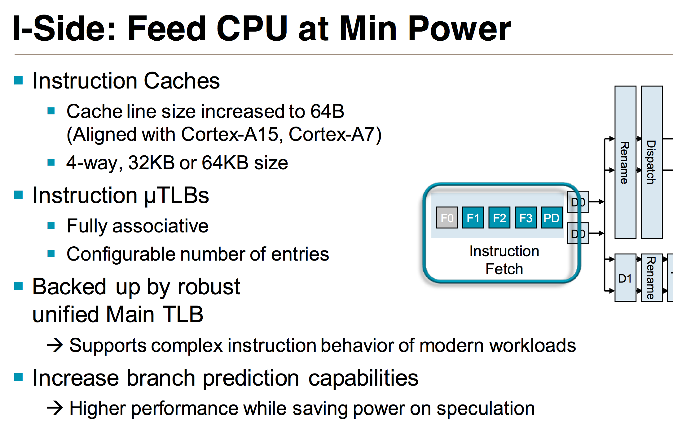
The L1 instruction cache is 4-way set associative and configurable in size (32KB or 64KB). The cache line size in Cortex A12 was increased to 64 bytes (from 32B in Cortex A9) to better align with DDR memory controllers as well as the Cortex A7 and A15 designs. Similar to Cortex A9 there’s a fully associative instruction micro TLB and unified main TLB, although I’m not sure if/how the sizes of those two structures have changed.
The branch predictor was significantly improved over Cortex A9. Apparently in the design of the Cortex A12, ARM underestimated its overall performance and ended up speccing it out with too weak of a branch predictor. About three months ago ARM realized its mistake and was left with the difficult situation of either shipping a less efficient design, or quickly finding a suitable branch predictor. The Cortex A12 team went through the company looking for a designed predictor it could use, eventually finding one in the Cortex A53. The A53’s predictor got pulled into the Cortex A12 and with some minor modifications will be what the design ships with. Improved branch prediction obviously improves power efficiency as well as performance.

Back End Improvements
The front end of the Cortex A12 is a bit more efficient than the Cortex A9, but the bulk of the performance gains really come from improvements to the execution side of the core. Similar to the Cortex A15, ARM introduced multiple independent issue queues ahead of the functional units. It’s important to get nomenclature right here. Instructions are decoded into micro-ops, renamed instructions are dispatched into the issue queues and then micro-ops are issued from the issue queues when their operands are available. Everything up to the issue queue is handled in order, while issuing can be handled out of order in the Cortex A12 (in most cases, more on this later).
Whereas the Cortex A9 had a single issue queue ahead of all functional units, the Cortex A12 moves to three independent issue queues. The A9’s issue queue could hold 4 decoded instructions, while each issue queue in Cortex A12 is larger than that. The move to larger independent issue queues alone should help with increasing IPC.
The three issue queues are as follows: one for integer, one for FP/NEON and one for loads and stores. ARM provided bits and pieces of an architectural block diagram for the Cortex A12. I reconstructed one as best as I could below. The blue blocks indicate in-order components of the design, while the pink/salmon blocks are out-of-order. You can toggle between the A12 and A9 diagrams to see how things have changed.
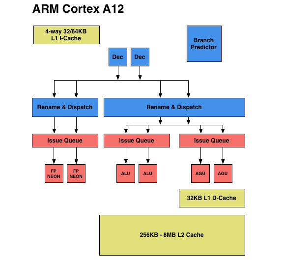
Cortex A12 retains the two integer pipelines of the Cortex A9, but adds support for integer divides (like the A7 and A15, other A-series architectures generally lacked support for hardware int divides). The rest of the integer execution capabilities are unchanged.
The FP/NEON units are vastly improved on the Cortex A12. When the Cortex A9 was first introduced, NEON code was rarely used which even lead NVIDIA to dropping NEON support altogether in Tegra 2. Times quickly changed as NEON code is widely used in Android and mobile applications.
The Cortex A12 design retains separate physical register files for integer and FP operations, but the RFs are larger than in Cortex A9.
Although Cortex A9 was considered an out-of-order microarchitecture, all FP and NEON instructions were executed in-order. With Cortex A12, ARM moves to a fully out-of-order architecture, at least as far as non-memory-ops are concerned. The FP/NEON issue queue now dual-issues into two FP/NEON pipes, both of which operate fully out-of-order. The FP/NEON pipes are also more tightly coupled, allowing for quicker data movement between FP and Integer units.
The improvements to the FP/NEON side are expected to show up quite nicely in benchmarks. ARM shared performance data using an FFMPEG workload on simulated Cortex A9 and Cortex A12 designs at the same frequency with the same number of cores (1):
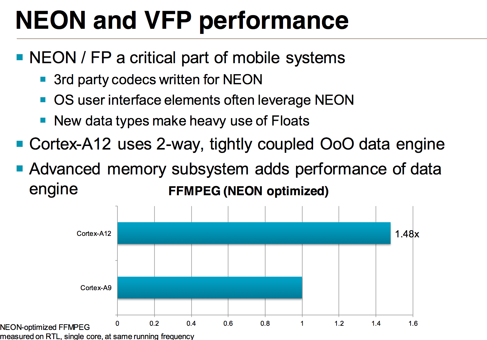
A 48% increase in NEON performance isn’t unexpected at all given the magnitude of improvements to this part of the execution engine.
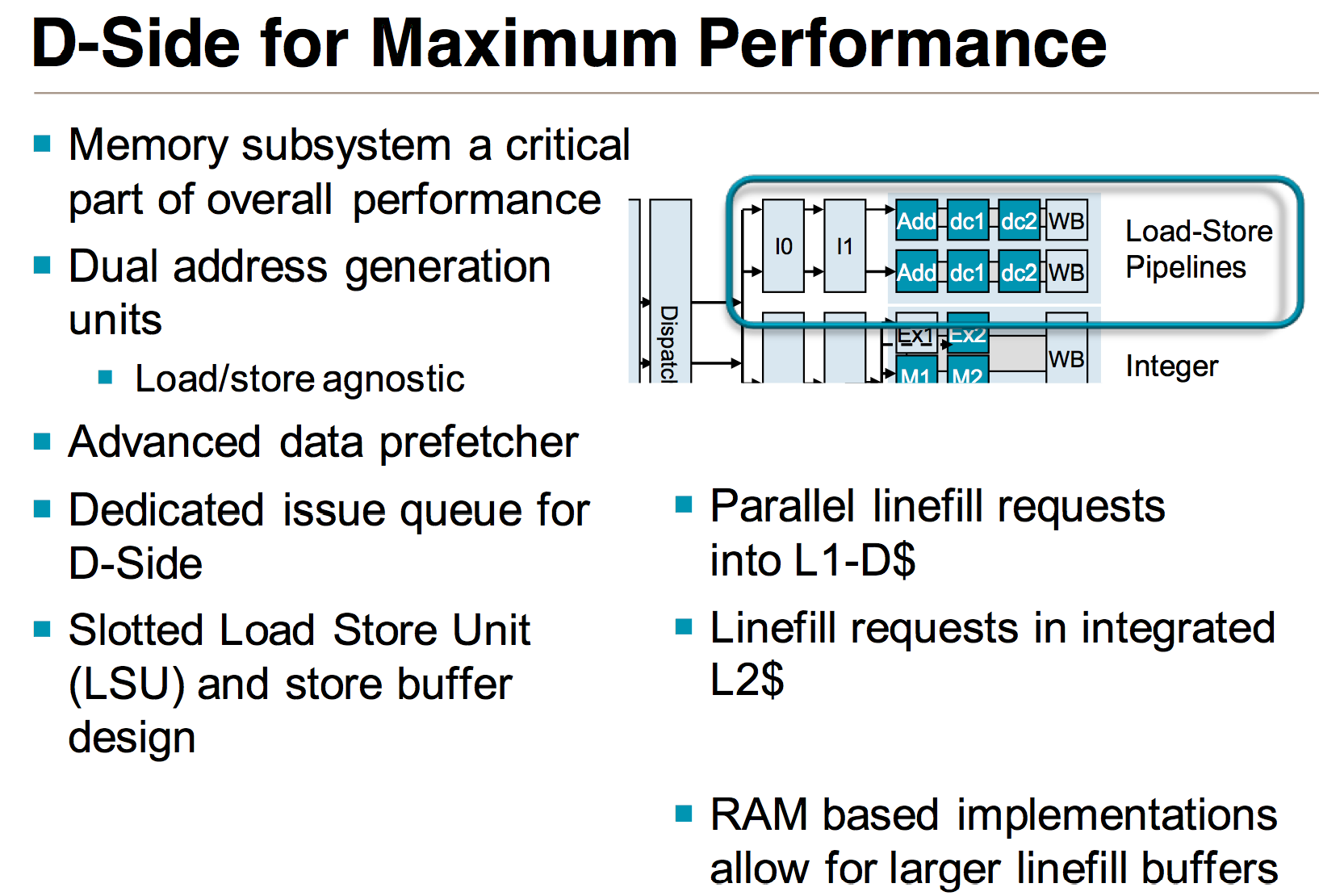
The final issue queue feeds the two load-store pipelines with two AGUs, once again a doubling from what was present in the Cortex A9 design. Each pipeline is equally capable (load/store agnostic) and mostly out-of-order (limits on what you can re-order if there are address dependencies between loads). By comparison, the load/store pipe in Cortex A9 was fully in-order.
Performance Expectations & Final Words
ARM’s Cortex A9 was first released to licensees back in 2009, with design work beginning on the core years before that. To say that the smartphone market has changed tremendously over the past several years would be an understatement. Many of the assumptions that were true at the time of the Cortex A9’s development are no longer the case. There’s far more NEON/FP code in use on mobile platforms, higher frequency of memory accesses and much heavier performance demands in general. While the Cortex A9 was a good design for its time, its weaknesses on the FP and memory fronts needed addressing. Thankfully, Cortex A12 modernizes the segment.

Although ARM referred to Cortex A9 as an out-of-order design, in reality it supported out-of-order integer execution with in-order FP and memory operations. ARM’s Cortex A12 moves to an almost completely OoO design. All aspects of the design have been improved as well. Although the Cortex A9 is expected to continue to ramp in frequency over the next year as designs transition to 28nm HPM and beyond, Cortex A12 should deliver much better performance in an more energy efficient manner.
At the same frequency (looking just at IPC), ARM expects roughly a 40% uplift in performance over Cortex A9. The power efficiency and area implications are more interesting. ARM claims that on the same process node as a Cortex A9, a Cortex A12 design should be able to deliver the same or better power efficiency. The design achieves improved power efficiency by throwing more die area at the problem; ARM expects a Cortex A12 implementation to be up to 40% larger than a Cortex A9. Just like the increasing performance of the Cortex A15 line of microarchitectures necessitates development of the Cortex A9/A12 line, the increasing size of this line drives up demand for the Cortex A7/A53 family below it.
ARM’s unique business model allows for the extreme targeting and customization of its microprocessor IP portfolio. If one of its cores gets too large (or power hungry), there’s always a smaller/more energy efficient option downstream.

The Cortex A12 IP has been finalized as of a couple of weeks ago and is now available to licensees for integration. The first designs will likely ship in silicon in a bit over a year, with the first devices implementing Cortex A12 showing up in late 2014 or early 2015. Whether or not the design will be too late once it arrives is the biggest unknown. Qualcomm’s Krait 300 core should provide the smartphone market with an alternative solution, but the question is whether or not the mobile world will need a Cortex A12 when it shows up. We always like to say that there are no bad products, just bad pricing. A more aggressively priced alternative to a Snapdragon 600 class SoC may entice some customers. Until then, the latest revision to the Cortex A9 core (r4) is expected to carry the torch for ARM. ARM also tells us that we might see more power optimized implementations of Cortex A15 in the interim as well.


